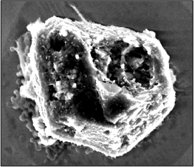
One of the first electronic materials, silicon carbide (SiC) is actually best known as an abrasive and the the majority of the worlds production is used as the black sandpaper you can buy in B&Q (or Home Depot for people in the states). Originally discovered in Sweden in 1824 by Berzelius (who was trying to make diamonds), it was Acheson who found the first production method for the manufacture of carborundum abrasives in 1893. Around this time Henri Moissan found grains of silicon carbide in the Diablo Canyon meteorite and hence the geological name for SiC is still Moissanite.
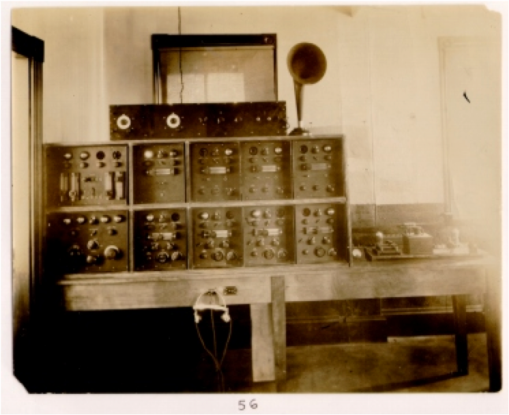
In terms of electronics, General Dunwoody used SiC diodes for radio detection in 1906 (US Patent 837616), as did Marconi for his transatlantic transmission in 1908.
Fast forward almost twenty years and carborundum detectors were commercially available.
The other device was an LED, which was discovered by Joseph Round in 1907. The second report wasn’t until 1923, when Lossev from the Nijni-Novgorod Radio Laboratory in Russia observed electroluminescence from SiC crystals.
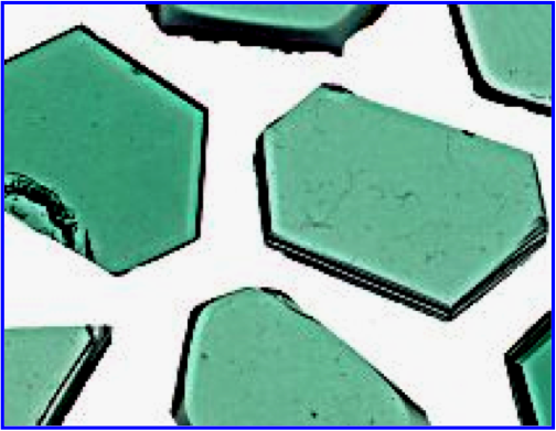
The big enabling step was the production of high quality crystals, the first of which came from Lely, who worked for Philips in 1955. Hexagonal in shape, these high quality crystals became the starting point for SiC research for a number of years and were used in the production of yellow LEDs in the 1960s.
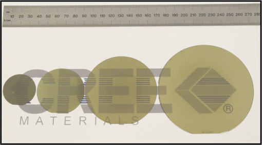
The next big step came from the Leningrad Electrotechnical University in collaboration with the Ioffe Institute, where Prof Tairov’s group published the first seeded crystal growth results. At the same time, epitaxy of SiC was started, with the work of Prof Matsunami at Kyoto, who manufactured the first 3C on Si MOSFETS. By 1987, Cree had formed from research undertaken at North Carolina State University, with 1″ wafers demonstrated by April 1989. The diameter of these wafers has increased and the micropipe density fallen rapidly in the intervening years, with Zero MicroPipe (ZMP) material launched by Intrinsic in 2006 (subsequently bought out by Cree) and the work of Nakamura who demonstrated Repeated A Face (RAF) growth in Nature in 2004.
Today, 6″ wafers have been demonstrated and will be in production in the near future. This opens up the market further, with a lot of existing 6″ process capability existing in the UK and that’s where the next summary will investigate, devices in SiC.


nice information